I may be wrong, but I would think you would want your CT referenced to ground. It might be ok to run your screens off of the balance resistor, but you could even be getting false readings for plate dissipation based on your ground reference.
In my research i found this reference design. CT reference point is between the stacked reservoir caps.
http://schematicheaven.net/fenderamps/twin_reverb_sf_135_schem.pdfI think if you reference the CT to ground, the ground reference of the rest of the design would also have to move to the intersection of the stacked reservoir caps to prevent shorting a PT secondary winding. But that would result in a dual rail power supply with +300V and -300V nodes.
These are the options:

Option D is the only setup that gives me the high voltage node and an acceptable screen supply voltage for EL34's.
I essentialy created the screen supply attached, but with the added balancing resistors.
I don't think these resistors pose a problem as they are also incoporated in the fender design above as 2x 100k 1W.
I also found this page (section 5 - Power supplies) an interesting read regarding all this:
https://sound-au.com/valves/design2.html#s5You could confirm by measuring current across your OT primary windings.
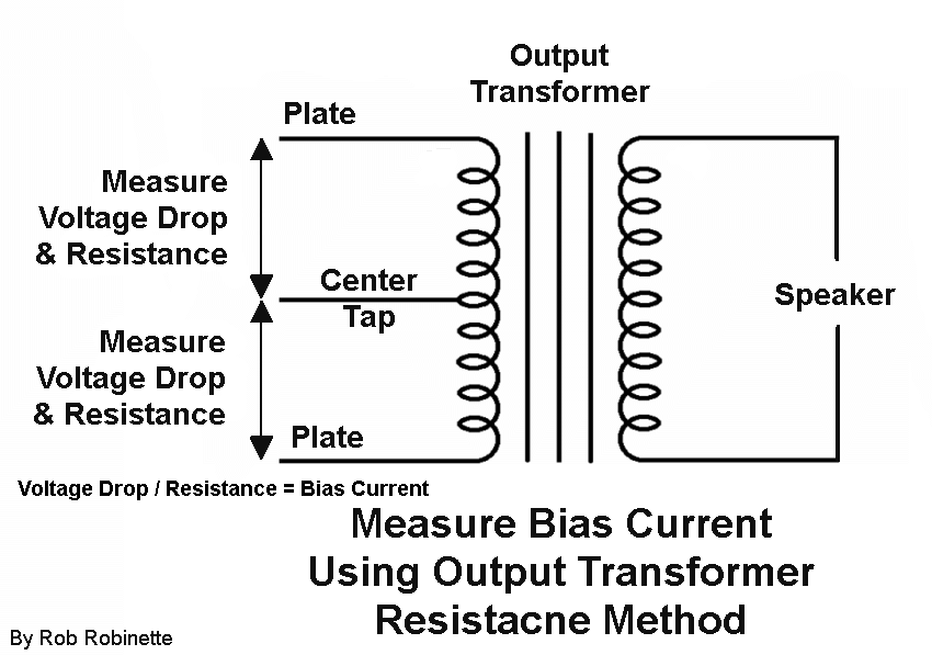
I will check bias with this method, i assume you are referring to this?
If you had a defective OT before changing the PS wiring, perhaps now with a good OT your voltages would be closer to stock with the original wiring.
No i did not, to be clear this is a new scratch build. I planned to use the available Conquest transformers i had lying around. The OT must have failed while in the Conquest and had not been tested during planning of this build. testing during build revealed it had a shorted winding to the core (and chassis) so i never used it.
In order to further experiment with the preamp voltages i might:
1. move the dropping resistors to the A node.
2. choose higher value dropping resistors for node C & D to drop the 590V to acceptable voltages for 12ax7 and EF86 tubes
3. maybe leave the 220k dropping resistor for node E as is for now and see where the voltage for V1 ends up
for 2. i would like to approach the voltages of the matchless design (+/- 415V), so i would need to drop 175V
with 2mA in the PI 12ax7 that would give me 175V / 2mA = 87k5 (82k? and dissipating 175V * 2mA = 0.35W
I think the ef86 has a max plate current of 6mA so: 175V / 6mA = 29k (27k?) and dissipating 175V * 6mA = 1.05W
these are not exactly standard values, any thoughts?

 Topic: Matchless Clubman build (Read 6187 times)